TSMC Hits Pause on ASML’s Newest Lithography for A13 Process

TSMC has officially hit pause on ASML’s newest lithography technology, a move that has captured the attention of the entire semiconductor industry.
According to Bloomberg, the chipmaking giant decided against purchasing ASML’s latest High-NA EUV machines for its upcoming process node, asserting that the capability is not yet required for its newly announced A13 technology.
This strategic pivot sent ASML’s shares lower and raised fresh questions regarding the timing, economics and competitive dynamics surrounding the world’s most advanced manufacturing tools.
The decision to skip the latest tech
ASML’s High-NA EUV systems are engineered to print the most intricate layers on leading-edge chips with higher precision than current EUV tools.
While companies like Samsung and TSMC already deploy standard EUV for complex layers and DUV systems for others, TSMC is choosing to wait.
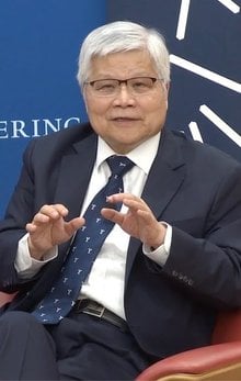
Co-Chief Operating Officer Kevin Zhang clarified that the A13 node does not necessitate the upgrade, suggesting a “defer-not-abandon” posture.
Bloomberg reports that TSMC may not adopt the technology until 2029, aligning the transition with a future node where cost-per-transistor benefits are more definitive.
Inside the A13 node and market fallout
TSMC describes A13 as a direct evolution of the A14 node announced in 2025, focused on enabling more compact and efficient designs for AI and high-performance computing.
Chairman and CEO Dr C.C. Wei emphasised that A13 is meticulously engineered for high-volume production exactly when visionary designs demand it.
However, the market reacted swiftly to the news of the delay – ASML’s shares dropped roughly 3%, representing a loss of approximately US$16.76bn in market value.
This comes at a sensitive time for ASML, which recently announced plans to streamline operations and implement recruitment freezes.
Despite the selloff, ASML remains Europe’s most valuable company, while TSMC’s US$1.8tn market cap underscores the massive influence its roadmap exerts on the global supply chain.
Economic and competitive implications
The choice to bypass High-NA EUV for the A13 node signals a complex cost-and-timing calculus.
High-NA promises tighter patterning but comes with significant costs and technical complexity.
By opting out for now, TSMC suggests it can meet near-term performance targets using existing equipment, potentially managing capital intensity and yield risks more effectively.
This creates a divergence in the industry: while rivals might adopt the technology earlier to differentiate themselves, TSMC is betting on a more measured path.
Plus, McKinsey notes that global chip supply chains are already under pressure from geopolitics and material constraints, making massive capital bets on next-gen tools harder to greenlight amid such uncertainty.

The road ahead
The ultimate timeline for High-NA adoption remains fluid.
While 2029 is the current projected window, intense customer demand for AI and HPC designs could eventually accelerate that schedule.
For the moment, the world’s leading chipmaker has signalled that the newest lithography technology is either too expensive or unnecessary for its immediate needs.
Whether this reflects superior process ingenuity or simple fiscal discipline, it marks a significant shift in the narrative of semiconductor manufacturing progress.
Company portals


Executives
C. C. Wei
CEO